Major differentiation to competition
The discovery of ferroelectricity in HfO2 provides two major categories of differentiation compared to competing memory concepts:
On the one hand, due to the very nature of ferroelectricity, FE-HfO2 provides all the advantages that are provided by the physical effect itself: Ultra-fast switching at the speed of sound, ultra-low power due to switching by field effect only (not current driven like MRAM, PCM or RRAM) and scalability due to its nature as a bulk switching effect.
Performance advantages of One-Transistor FeFET memories:
Even though there are nowadays many emerging memory concepts sampling or close to product stage, none of these concepts fulfills the requirements that are relevant for the age of Internet-of-Things (IoT): Low power, high performance and at the same time low in manufacturing cost.
- One-transistor (1T) FeFET memories show femto Joule write operation due to the fact that memory states can be written by application of an electric field alone. This is completely different from established embedded Flash or any other emerging memory concept and therefore provides at least a factor of 1000 improvement in per bit write energy.
- Due to the fact that switching of the binary states in FeFET memories is based on ferroelectric polarization reversal, the speed is governed by the movement of the ions in the crystal lattice. Since this is determined by the speed of sound, it translates to nanosecond switching speed for the 1T FeFET.
- Since 1T FeFET memories are actually derived from standard HKMG logic transistors, the concept is inherently scalable alongside the CMOS baseline. The scalability is the fundamental enabler for keeping manufacturing cost low, i.e. the chip area consumed by the nonvolatile memory as small as possible.
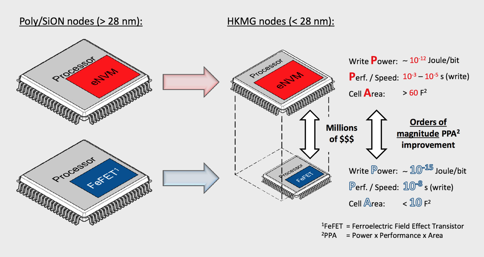
The combination of these three attributes is often summarized in the power x performance x area product that is unchallenged for FeFET-based memories. Especially for embedded memories, which are highly relevant for the age of IoT, this differentiation is again illustrated in Fig. 5.
Besides these most striking advantages, ferroelectricity in itself provides the most radiation hard memory effect on the market. This is especially important for segments like medical-IoT where memories have to fulfill stringent requirements in this respect. Moreover, the ultimate temperature stability of the memory concept is determined by the Curie temperature TC of the material. Since it has been reported that TC of ferroelctric HfO2 is above 450°C, the FeFET can in principle address even the automotive segment which is subject to very stringent reliability requirements.
Embedded capability
Besides the performance advantages that are intrinsic to one-transistor FeFET memories, the fact that FeFETs can be derived from HKMG transistors is ideal for embedding memory cells next to logic transistors. Following properties highlight the embedded capability of FeFET:
- Low mask adder to embed FeFET besides HKMG
- Negligible process adder to CMOS baseline
- Reflow capability of FeFET
- No new materials introduced into CMOS manufacturing
All these properties have already been verified on a 28 nm gate first process flow of our partner GLOBALFOUNDRIES. Embedding FeFET into HKMG does not alter logic device performance in any way.
Scalibility to future nodes
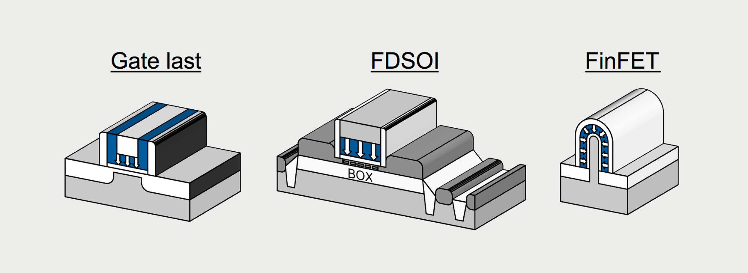
Once again, due to the fact that FeFET memory cells can be derived from transistors utilizing hafnium oxide, the scalability of the concept can be provided down to 1X nm nodes and beyond. FeFET memories based on gate last, FDSOI or FinFET processes are simply the next logical step (Fig. 6). Due to the fact that ferroelectric HfO2 can be deposited by atomic-layer-deposition (ALD), more complicated transistor or capacitor structures (FinFET, trench or stacked capacitors) utilizing ferroelectric HfO2 can be realized.

Fig. 5: The FeFET concept compared to other embedded nonvolatile memory (eNVM) when scaled from Poly / SiON technology nodes down to HKMG. The unique combination of power x performance x area attributes positions the concept as the ideal solution for semiconductor chips addressing the Internet-of-Things (IoT).
Fig. 6: Illustration of the scalibilty of FeFET memory cells. Due to the conformal deposition properties of ALD, more complicated CMOS processes like gate last or FinFET can also benefit from the concept. FDSOI nodes are ideally suitable for embedded FeFET memories due to their focus on leveraging performance and cost for IoT applications.